M-EP1
This project has brought me many new insights. I want to use this blog post to record my thoughts and learning throughout the process, and hopefully provide some reference for friends who are interested in creation.
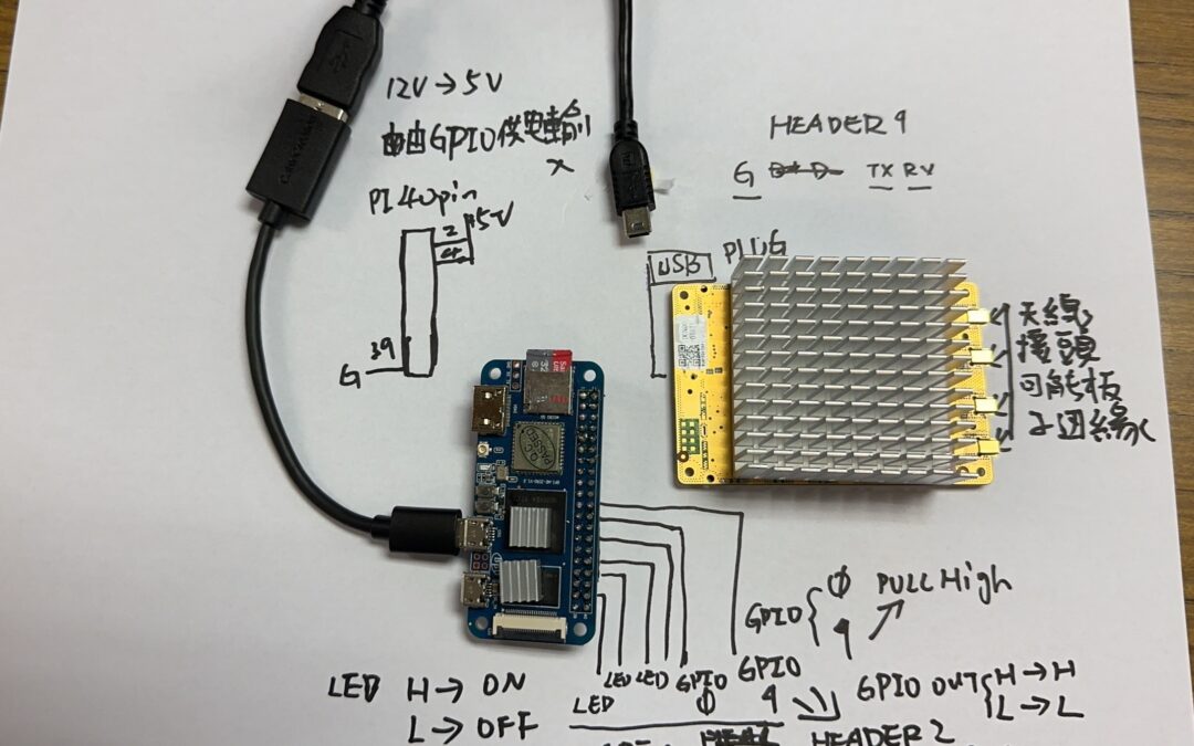
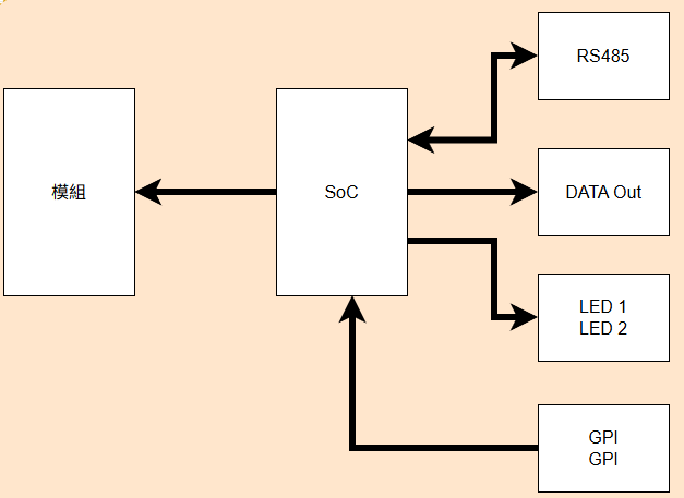
The starting point was actually quite simple. One day, my boss assigned me a task: "There's a module that needs control, and maybe in the future, it could become our own product!" Upon receiving this instruction, I followed my usual habit and quickly sketched my ideas on paper, outlining a preliminary concept diagram (as shown below).
To be honest, the last time I designed a circuit board, SMD components hadn't yet become mainstream. It was then I realized that I had somewhat fallen behind the latest developments in the industry.
Nonetheless, I've been keeping an eye on related communities over the years. During the pandemic, I attended several online sharing sessions, listening to passionate Makers showcase their creations. Suddenly, the name "Guan Shuai" popped into my mind. Although I am more of an introverted person, this time I decided to take the initiative to contact him and discuss my amateur sketch.
Frankly speaking, professionals would probably look at this sketch and think, "What on earth is this?" But to achieve the goal, I had no choice but to push forward! This marks the beginning of the first version of the SoC design! (Sensitive information has been removed.) M-EP1
M-EP2
After this starting point, I deeply realized that the smooth progression of a project must be built on trust among partners. Only through mutual trust can we foster good interactions and efficient collaboration.
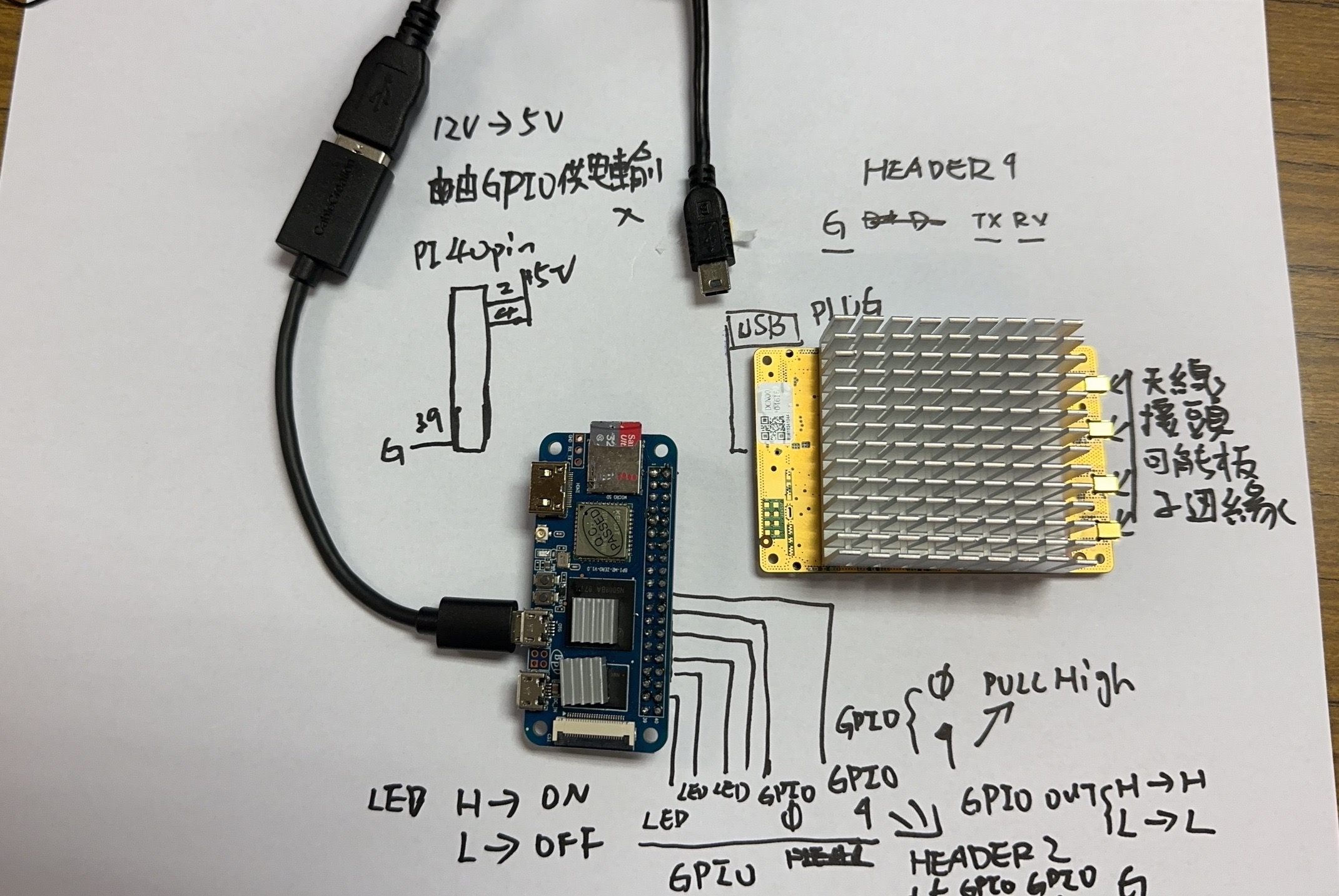
Soon, the concept that was originally just a hand-drawn sketch rapidly evolved into a basic 3D rendering thanks to the strong execution capabilities of our outsourcing team. Of course, this was merely the starting point for communication, not the endpoint of the project.
Since the project was initially in the conceptual stage, there wasn't even a formal specification document. All ideas had to rely on my imagination to fill in the gaps. On the other hand, the client's requirements were also undecided, and information was relatively unclear. Therefore, under such circumstances, I could only use my experience and judgment to turn the imagined blueprint into practice. M-EP2
M-EP3
A good start is certainly important, but the key to successfully completing a project lies in "perseverance." At this stage, my outsourcing partner and I had silently formed a small and agile team, all working cohesively toward the same goal.
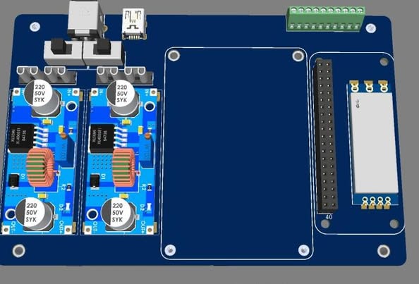
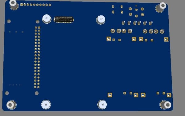
We decided to adopt a B2B modular approach to circuit design. This decision was partly because the module we initially connected was already using this concept, and we hoped to shorten the initial verification time. Looking back, this choice indeed saved the project a lot of time and accelerated subsequent development progress.
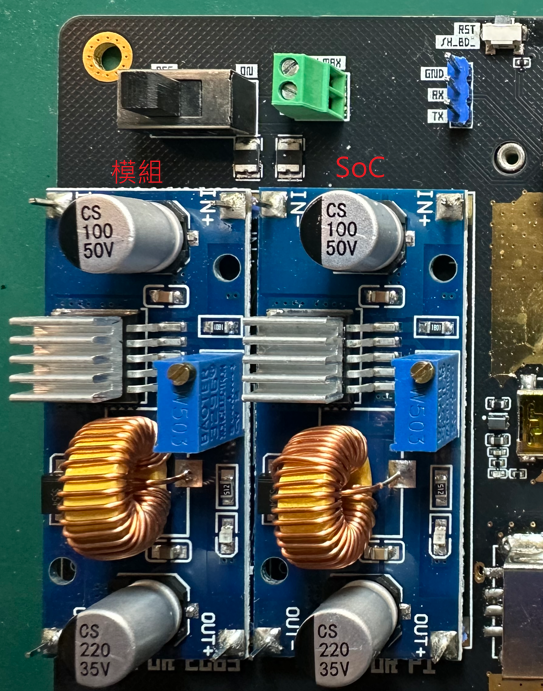
However, the first technical challenge we encountered was the design of the power supply specifications. According to the requirements, the system needed to accept DC 12V input and simultaneously provide 5V power to both the module and the SoC board. To avoid interference between the two, we decided to use a dual power supply design, allowing each module's power to operate independently. This way, even if one side encounters issues, it won't affect the operation of the other module. M-EP3
M-EP4
After solving the power supply needs, the next issues were more challenging. This time, the main module adopted specific connectors and fixed hole positions, but initially, we didn't have complete dimension diagrams. We had to rely on experience and on-site measurements. Honestly, this "no diagram to refer to" situation was a bit stressful for me, as getting it right in one go was not easy.
Even more awkwardly, the measurement work had to be completed on my end first, and then all the data handed over to the partner for hole positioning. This process really tested mutual trust because if one step went wrong, the entire design would fall apart. For those who often handle such projects, this might be just a routine matter, but for me, every time felt like a precision challenge.
Fortunately, just as we were about to send the PCB for fabrication, we finally received a more accurate CAD diagram. At that moment, I breathed a sigh of relief and quickly compared our measured data with the CAD diagram. The results showed minimal error, which was exhilarating—our measurements were completely accurate!
That was a truly rewarding moment, and we successfully completed the precise alignment of the board.


M-EP5
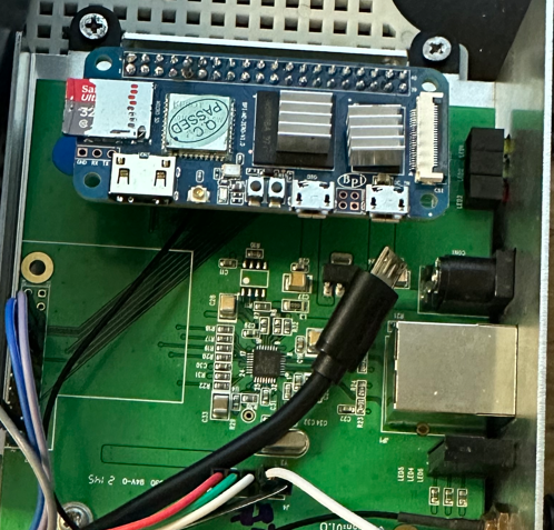
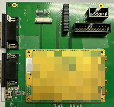
While discussing hardware, the software side was also actively working. This time, we reused a previous baseboard, connected the SoC to it, and then linked it to the manufacturer's Demo Board via USB. This board had been used before, and its operation was similar to a standard SoC board. Essentially, we treated it like a Pi Zero; connecting it with an OTG cable made it functional.
However, when it comes to software development, that's another story to share slowly. For now, let's wrap up the first phase of hardware discussion and leave the software challenges for later. M-EP5
M-EP6
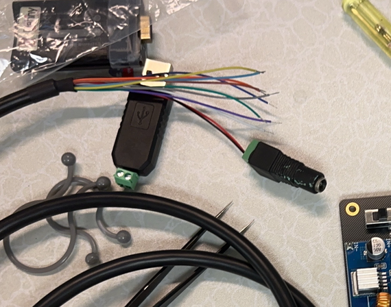
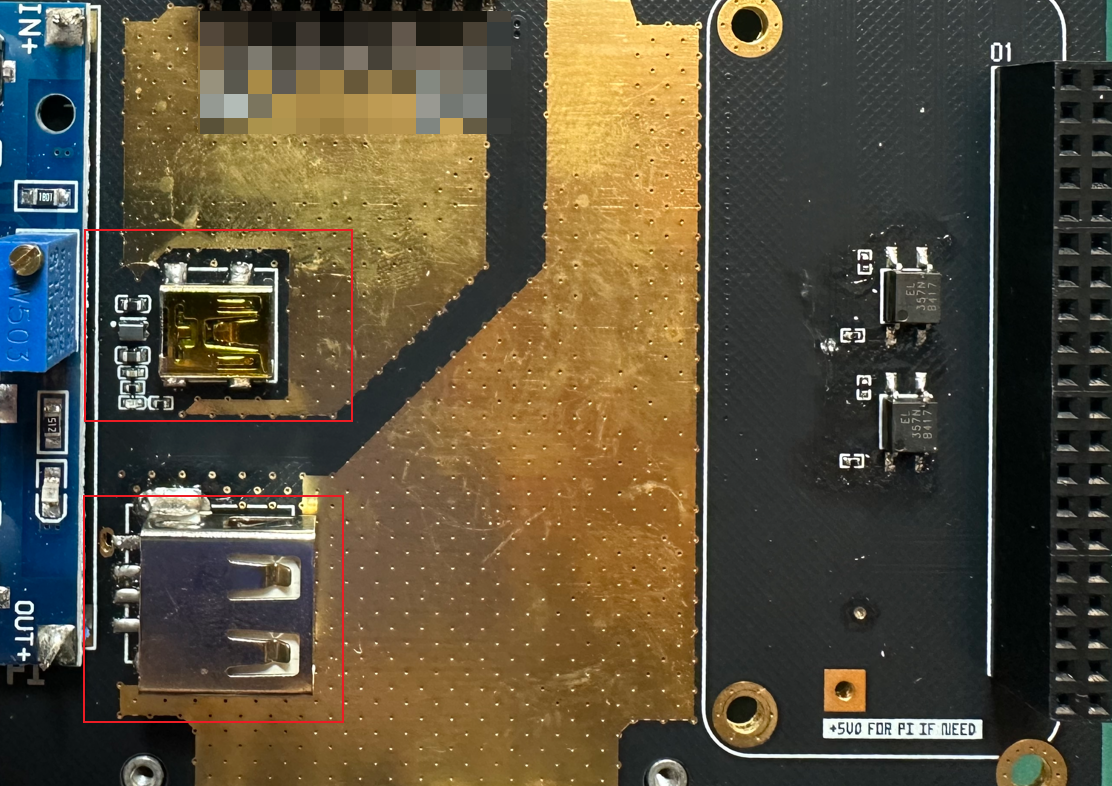
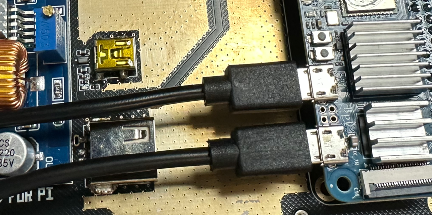
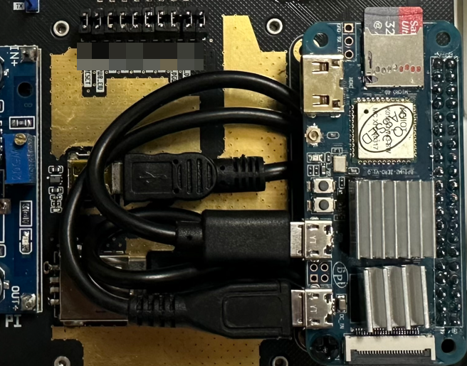
M-EP6 After overcoming one challenge after another, we faced the next hurdle: connecting the module's USB and SoC's OTG transmission cable, as well as the SoC's power transmission line. Although they were all USB cables, the connectors varied, including Type A to Micro USB and Mini USB to Micro USB. Ultimately, we opted for adapter cables to solve this issue.
The main board required USB connectors, and at this point, we had to consider the routing distance between the connectors. It couldn't be too short or too tight. After evaluation, although the appearance wasn't the most ideal, this approach at least allowed us to achieve our goal successfully.
M-EP7
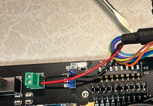
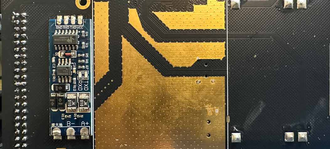
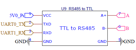
M-EP7 After solving the most troublesome issues, there was only one internal connection left—the RS485 output interface. To avoid the hassle of controlling RS485's DE/RE signals, we opted for an auto-switching module this time, which saved us a lot of effort and proved to be incredibly useful!
However, since the module itself was quite large, we had no choice but to place it on the back of the board. Fortunately, after connecting TTL UART's Vcc, TXD, RXD, and GND, RS485's output only required A+, B-, and GND, making the wiring relatively straightforward.
With this, all the modules needed for the board were finally completed. Although the overall design might seem like simply "stacking modules," every step had to be meticulous. After all, PCB fabrication only gives you one chance, and every decision had to be tested with actual module connections before proceeding. Ultimately, the workload was still quite substantial.
M-EP8
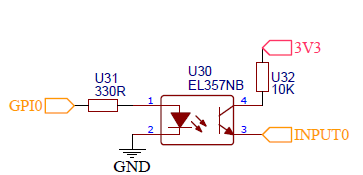
M-EP8 With most of the hardware functionality decided, the next task was to design a control line. This line served a simple purpose: when +12V voltage was input, the software could detect the signal and activate internal functions, similar to the Enable pin on an IC—providing a high level to initiate action.
But there was a problem: the SoC could only accept +5V or +3.3V voltage, so directly connecting +12V was out of the question. Faced with this mismatch, we decided to use a common optocoupler switch to solve the issue. When GPIO provided a positive voltage, the optocoupler conducted, connecting pins 4 and 3, allowing INPUT0 to receive +3.3V. This safely transmitted the signal to the SoC's input pin, achieving a high level effect.
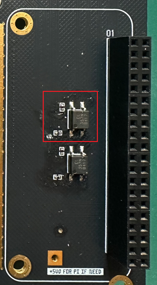
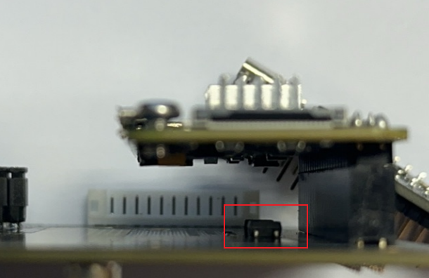
Interestingly, we managed to cleverly fit the components into the space between the SoC and the baseboard, making the overall layout more compact without taking up too much space.
M-EP9
After several rounds of assumptions, repeated verifications, and circuit testing on breadboards, we finally finalized the circuit design. With this, the board design for the entire product was nearing completion.
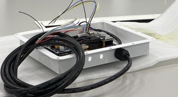
From the beginning, we planned for this board to be installed in an integrated mechanism, where all inputs, outputs, and power would be consolidated into one multi-core cable. Ultimately, we only left one LED indicator for status identification—simple and clear.
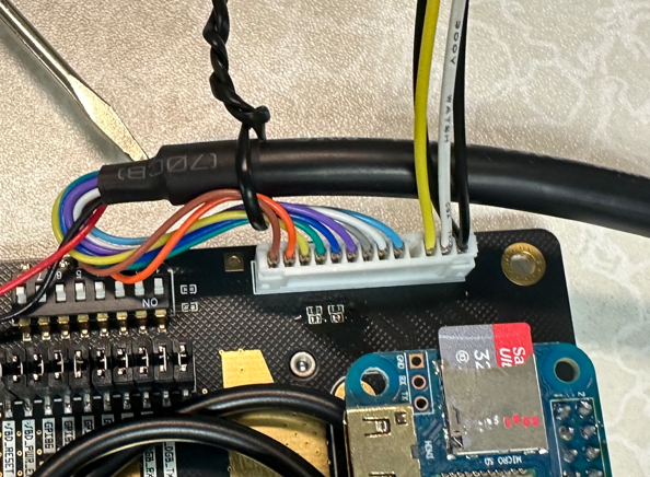
This development taught me an important lesson: "custom cable manufacturing" costs are much higher than I initially thought. For example, when selecting terminal connectors like PH2.0 male and female connectors, it's best to use common pin counts (2, 4, 6, 8, 10) to make procurement and inventory management more reasonable. However, I overlooked this detail and chose a 13-pin specification, which is rare in the market, causing significant difficulties in subsequent material preparation.
Additionally, when working with fabricators, it's crucial to identify potential errors in the production process during the design phase and avoid such issues as much as possible. Although this version is ready for mass production, it might not be the most ideal choice for reducing production costs and error rates.
